A Seven-Year-Old Chip Startup Just Raised $468 Million to Fix the AI Memory Shortage
Kepler Computing says it can squeeze more memory into existing chip factories, skipping the $20-to-$40 billion cost of building new ones. What that means for the AI bottleneck holding back everything from data centres to your favourite apps.
Key points
- Kepler Computing, founded in 2018, emerged from stealth this week after raising $468 million from backers including Intel Capital, AMD Ventures, GlobalFoundries, Baillie Gifford and Gates Frontier.
- The US Department of Commerce committed up to $245 million in July to help Kepler build high-performance AI memory technology inside the United States.
- Kepler's approach skips extreme ultraviolet lithography, an expensive chip-printing technique, and instead uses new materials and 3D stacking to pack more memory into existing factories.
- The startup plans to ship its first sample chips later this year, scale production in Singapore in 2026, and begin US chip production in 2028.
- Kepler has tested its process on roughly 2,000 wafers so far, a small number compared to the millions a full-scale factory would need.
Memory is often the culprit when an AI chatbot takes a second too long to answer or a data centre hits a processing wall. Not memory in the abstract, but the physical chips that hold data while processors work through it. The world doesn't have enough of the fast, dense kind that AI systems need, and building more from scratch costs tens of billions of dollars. We looked at the downstream pressure this shortage creates when we covered Google forcing Android apps to use less memory on 27 August.
Kepler Computing thinks it has a faster, cheaper path.
What is Kepler actually doing?
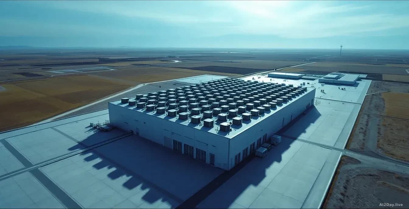
Kepler isn't building new chip factories. It's retooling existing ones to produce a better grade of memory, and it came out of stealth this week after seven years of quiet development, as first reported by Wired AI.
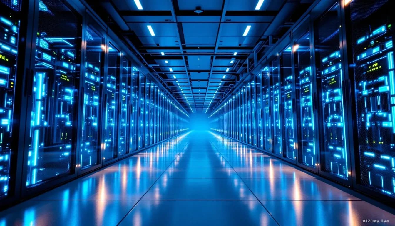
The target is high-bandwidth memory, or HBM: the fast lane between a computer's processor and its data. AI models need enormous volumes of data delivered at very high speed. HBM does that job, but demand has outrun supply.
Typically, chipmakers use extreme ultraviolet lithography, or EUV, to print fine patterns onto silicon. EUV machines cost hundreds of millions of dollars each. Kepler says it can achieve similar density without EUV, using 3D stacking (layering memory chips on top of each other rather than spreading them flat) alongside a composite material built around ferroelectricity, a property that lets data be read and written at lower power than conventional methods. The team ran through 35 versions of that composite before settling on one they believed would hold up at scale.
Who is backing this, and how much?
| Backer | Amount / Role |
|---|---|
| Intel Capital | Investor (amount undisclosed) |
| AMD Ventures | Investor (amount undisclosed) |
| GlobalFoundries | $50 million investor and manufacturing partner |
| Baillie Gifford | Investor (amount undisclosed) |
| Gates Frontier (Bill Gates) | Investor (amount undisclosed) |
| US Dept. Of Commerce | Up to $245 million in committed funding (July 2026) |
| Total raised | $468 million |
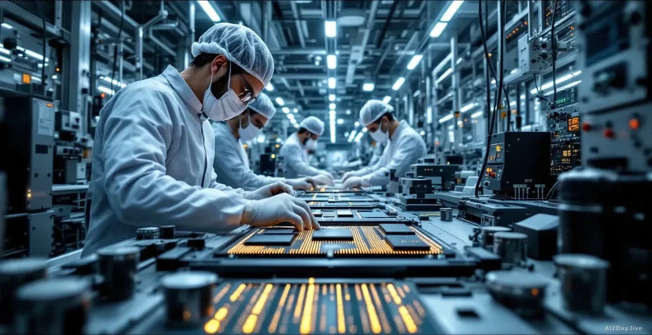
GlobalFoundries, a major chip manufacturer with facilities in Singapore and Burlington, Vermont, is both a financial backer and the factory partner where Kepler runs its tests. Kepler says it converted one of those facilities into a next-generation memory fab in eight months. A normal conversion takes about 24 months.
Should investors and ordinary people get excited yet?
Not too fast. Kepler has processed roughly 2,000 wafers, the disc-shaped silicon sheets from which chips are cut. A commercial factory churns through millions. Getting consistent results at that scale is where many promising chip startups have stalled.
There's also a practical materials problem. Kepler's composite contains iron, a well-known contaminant in chip production. Iron particles can ruin an entire batch of wafers if they escape into the production flow. GlobalFoundries says Kepler's process must run on dedicated equipment, fully separated from other production lines.
The science appears to work in the lab. Making it work reliably and in quantity is the harder test.
For ordinary people, the payoff would be AI tools that run faster and cost less to operate, because the companies running them spend less on specialised memory. That's a real benefit. But 2028 is the earliest realistic date for US production, and the comparison that matters is the $20-to-$40 billion cost of building a new fab from scratch.
What happens next?
Kepler plans to ship its first HBM sample chips to potential customers before the end of 2025. Volume production in Singapore is targeted for 2026. US production is pencilled in for 2028, supported by the Department of Commerce funding.
My read: the sample chip timeline is the only number worth watching right now. Big orders from chip buyers after testing would be the real signal that this works outside a controlled environment. The fundraise is large and the backers are credible, but Kepler is still orders of magnitude away from production scale, and iron contamination is a solved problem only on paper so far.